














Our Open-Q 5165RB SOM and G520 Gateway in Action
Vision Intelligence At Embedded World 2022, we are displaying the Open-Q 5165RB development board powered by Q…

Built for how enterprise networks work today.
Lantronix Centralized Management Software
In today’s digital design world, speed is almost always the main factor determining the performance of the product. Every design is packed with a few to many high speed interfaces with signal speeds high enough that the traces and layout of the printed circuit board (PCB) play a significant role in the overall system performance.
Consequently, signal integrity and power integrity issues tend to be the main causes of device failure in various design stages of the product. It is prudent for the design engineer to give careful consideration to the analog characteristics of a high speed PCB design in addition to the digital parts. Any physical phenomenon that may increase timing uncertainty of the digital waveform must be accounted for in the design.
This article presents the basic design concepts of signal integrity (SI) and power integrity (PI) in high speed PCB and hopes to provide practical tips in PCB design.
SI is achieved when well-defined PCB paths are implemented. These paths allow for signals to be delivered from the driver to the receiver with a clean edge at the right timing. A design with poor SI often does not meet timing or jitter requirements. In some cases, a poor SI may also cause higher than acceptable radiated emissions. In the worst case scenario, the design does not function.
The important design considerations to achieve high speed SI are as follows:
In the early days of electronics, SI is not a concern due to slower edge rate. As clock rate and signal speed increases, the rise time consequently reduces to the point where the length of the PCB traces are on the same order of length as the edge rates passing them. For an HDMI 1.4 signal data rate of 2.97Gbps, the critical PCB length is at 2mm. As such, transmission lines of high speed PCB and their characteristic impedances, delays, and losses need to be carefully analyzed. These transmission line behaviors are key to determine how the connected components interact. The most common transmission line impedance to achieve is 50OHM.
Communication with PCB fabrication houses determine the PCB material, stack up, and identification of the trace width/clearance in each layer to meet the required impedance.Two common types of transmission lines used in PCB design are stripline and microstrip. The stripline has the signal trace sandwiched between two reference planes. Microstrip has the signal trace routed on the outer layer and has only one reference plane. The selection between the two depends on the signal speed requirement, the complexity of the design, and the fan-out arrangement from the driver IC. In general, stripline is less susceptible to noise and microstrip offers faster signal speed path.
Once PCB material, stack up, and transmission line type are defined, the designer needs to decide how the high speed signals are routed. When considering the signal trace, it is important to pick a clean and short trace with an undisrupted reference plane underneath. This allows current to travel to the receiver with consistent impedance and return to the source through the path of least impedance, which is the reference plane directly adjacent to the signal trace. The common return path problems include (a) when there is a discontinuity in the reference plane and (b) when the routed signal changes layers with no reference plane to follow underneath. The consequences of the above mentioned disrupted return paths are signal reflections and ringing.
Signal reflections and ringing are the direct results of poor signal integrity design. The driver, the transmission line, and the receiver impedance all could lead to signal reflections. If a signal encounters a change in the instantaneous impedance of the PCB as it propagates down, part of the signal will reflect back to its source and cause signal distortion. The change in this instantaneous impedance is called impedance discontinuity. Ringing arises when multiple reflections are present due to impedance discontinuity. If the driver, the interconnect transmission line, and the receiver are of the same impedance, there would be no reflections or ringing. Therefore, matching the same impedance between the components and interconnects is the key to reduce ringing.
Cross talk is the result of signals coupling due to the capacitive and inductive nature of the PCB traces. Cross talk can be caused by multiple signals coupled to one another from being routed too close or having signal return paths too close to one another. Crosstalk can be minimized when the routed trace and return paths are 2x the trace width away from the other signal traces. Ringing also contributes to the possibility of cross talk. Less ringing translates to less cross talk.
The termination topology, the lengths of the traces, the propagation speed of the signals, and the shape of the traces all needs to be considered. These are not discussed in this article.
Practical Design Rules to follow to maintain SI:
Power Integrity is achieved by providing a power delivery network (PDN) inside a system that complies with the required power supply conditions of the processors and all other components. PDN is a chain of interconnects in the form of transmission planes that deliver power from a voltage regulator module (VRM) through the PCB, across the package, and through the on-die routing to the transistors themselves.
PI is a much more complex concept to visualize compared to SI. This is demonstrated by the fact that there are tens and hundreds of nodes connected in the same power plane and every node affects the overall impedance in the PDN while SI deals with only the driver and the receiver. PI problems are difficult to repeat and troubleshoot. Therefore, a complete PI study in pre-layout and post layout PCB design stages are suggested. While an advanced and usually expensive PI simulation tool is required for a complete PI analysis, this article briefs the design fundamentals.
A good PI system in a high speed digital design serves two essential purposes. First, it provides stable voltage references (Ground/return path) for exchanging signals. Second, it distributes power to all logic devices with acceptable noises and tolerances to keep the voltage across the chip pads constant.
It sounds simple, but a few facts need to be realized in the high speed PCB design. First, there are typically hundreds of power and ground balls from a typical BGA processor which requires tens of power supply voltages. Second, all of these power pins consume many Amps of current. Consequently, when the device is in operation, all these power pins, that consume Amps of current, load all the power supply voltages at high frequencies simultaneously.
Taking the above facts into consideration, PI study is no longer just a purely DC analysis but involves the studies for transient loading at high frequencies in every power rail from the VRM to the IC pad.
1. Transmission Plane Behavior in High Frequencies
Similar to SI’s transmission lines, the key in PI analysis is treating all power rails as transmission planes and analyzes their characteristic impedances. To achieve good power integrity, it is desirable for the PDN to have the lowest impedance possible. High frequency transient noises can be generated and can propagate to the whole board if overlooked. The main challenge is that the PDN interconnects in the PCB all have an inductive nature. Component mounting, PCB traces, capacitors, and vias, all exhibit inductance. This suggests that impedance increases as the transient frequency increases. As the VRM, capacitors, PCB stack-up, power/ground plane, and the IC all have different characteristic impedance in different frequencies, careful selection of components and placement locations are the ways to reduce transmission plane impedance.
Two figures are shown below to demonstrate a capacitor’s inductive nature in high frequencies and the equivalent circuit for a typical PDN.
Figure 1 is an example of a 0603, X7R, 1uF capacitor’s impedance vs. frequency plot using AVX’s SpiCap simulation tool. The left half of the plot shows that the capacitance dominates the characteristic impedance between 0-22.5MHz and the right half of the plot shows that the inductance dominates the characteristic impedance for frequencies greater than 22.5MHz.
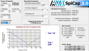
Figure 1. Example of a 0603, X7R, 1uF capacitor’s impedance vs frequency plot.
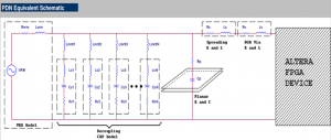
Figure 2 is a PDN equivalent circuit illustrating the resistive, capacitive, and inductive nature of each interconnect of the same transmission plane. All these physical phenomenon require thorough study as a part of PI analysis.
2. Target Impedance
Ideally, we want to keep the impedance throughout the transmission plane as low as possible.
As there are many factors impacting the impedance, target impedance needs to be calculated separately and independently for each voltage rail to all chips on the board. In each rail, the target impedance may vary with frequency due to the specific current requirement of the chip.
The impedance and acceptable tolerance information for each rail listed in the device specification sheet shall be used as starting guides when designating target impedance.
3. PDN Interconnects
As already described and shown in Figure 2, the PDN for a particular transmission plane consists of different interconnect blocks:
VRM -> bulk decoupling capacitors -> the vias -> the traces -> the planes on the circuit board -> additional decoupling caps -> the solder balls or leads of the packages -> the interconnects in the packages -> the wire bonds and the interconnects on the chips.
Each interconnect block contributes to the characteristic impedance of the transmission plane. When analyzing the PDN, it is important to study each interconnect rail first, and then the transmission plane, and then as a whole PDN system.
To illustrate how different each PDN interconnect affects the characteristic impedance of the same transmission plane in different frequency bandwidths, the ALTERA PDN Design Tool is used in example below. Start the design process by setting the target impedance to 12.3mOHM, and then go thru each PDN interconnect.
Note: the ALTERA PDN Design Tool can be downloaded with a valid Quartus II software license manufactured by Altera Corp.
A. VRM (DC-10kHz)
The low frequency impedance ranging from DC to 10 kHz is set by the VRM. The output of a typical VRM is typically in the order of mOHM from DC to 10kHz.
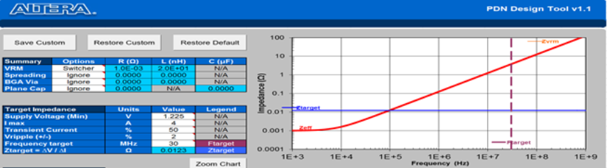
Figure 3 VRM characteristic impedance
Practical tips to consider for a VRM PCB layout:
B. Bulk Capacitors (10kHz-100kHz)
The bulk capacitors added in parallel to the VRM lowers impedance between 10kHz to 100kHz.
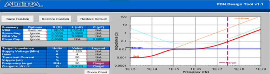
Figure 4 Bulk Capacitors characteristic impedance
Practical tips for selecting the right bulk capacitors:
C. Ceramic Decoupling Capacitors (100kHz-10MHz)
Decoupling capacitors lower the transmission plane’s impedance from100kHz to 10MHz. Add decoupling capacitors close to the entry points of the power pad reduces the loop inductance. Picking the right location and selecting the right number and value of the decoupling capacitors play an important part of this step.
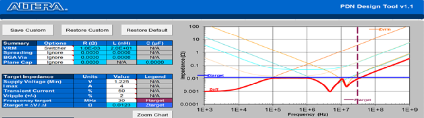
Figure 5 Decoupling Capacitor characteristic impedance
Practical tips to select the right decoupling capacitors:
D.PCB Power/Ground Planes (10MHz-100MHz)
A very closely stacked power and ground improves the characteristic impedance of the PDN between 10MHz-100MHz.
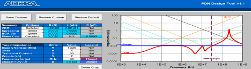
Figure 6 PCB Power/Ground Planes characteristic impedance
Practical tips for designing power/ground plane
E. BGA vias, IC Packages, on-die capacitance (>25MHz)
In general, for frequencies above 25MHz, the characteristic impedance is dominated by the vias to the BGA ball, IC package, and the on-die capacitance. To model this, a more advanced simulation tool is required.
F.Other notes on decoupling caps and power/ground planes
With higher clock rates and signal speeds in every digital design, attention to SI and PI is crucial in designing a well performing product. This article described some of the basic and fundamental considerations and practical tips pertaining to achieving SI and PI. Although this article explained SI and PI as separate topics, PI and SI are closely related and their issues can influence one another. Furthermore, a high speed PCB with carefully SI and PI design considerations usually has minimum electro-magnetic interference issues. Utilization of these practical tips in this article will equip engineers to design a successful product.
Author Chris Yao
Lantronix
About Chris Yao
Chris Yao is currently a senior hardware design engineer at Lantronix, where he works with software engineers and customers to define and develop cutting edge electronic products. Since joined Lantronix in 2014, he has been working on Qualcomm’s Snapdragon solutions in various projects. As a team member of the hardware group, he specializes in high speed digital design. Before Lantronix, Chris has been involved in analog and digital product designs for over 10 years.
Vision Intelligence At Embedded World 2022, we are displaying the Open-Q 5165RB development board powered by Q…
Welcome to the new home of Net2Edge.com. We are pleased to be joining our friends and colleagues from Transiti…
Built for how enterprise networks work today.
Lantronix Centralized Management Software